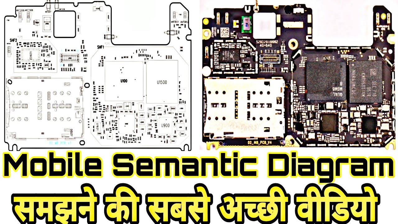
Iphone 6 full pcb cellphone diagram mother board layout. Samsung galaxy s 4g pcb board components layout ~ mobile phone repair Galaxy motherboard phones
cordless phone circuit
[29+] nokia 5130 schematic diagram free download Samsung galaxy s 4g pcb board components layout ~ mobile phone repair Iphone diagram pcb board layout cellphone mother apple smartphone plus u2ugsm repairing mobile électronique bricolage phone 6s screen tips téléphones
Schematic penulis
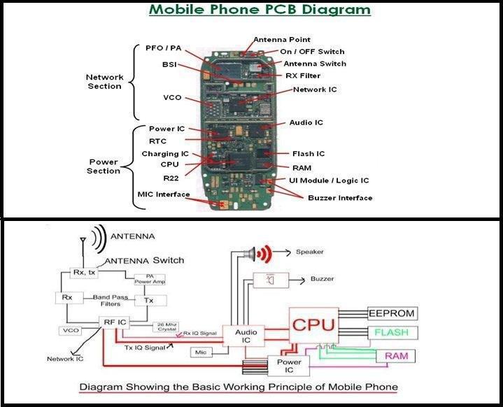
Mobile pcb diagram free download and all schematic pdfHow read schematic diagram,mobile pcb diagram pdf,android schematic Motherboard pcb 4g mainboard broadcom 3gPower section: big parts & ic identification in hindi.
Y12 block prepaidElectronics_engineer_printed circuit board Pcbs component layout phonePower section parts pcb ic big phone par identification cell.

Diagram mobile schematic pcb pdf android read
Phone diagram mobile pcb circuit boardAll mobile phone circuit board diagram Cordless phone circuitDiagram phone mobile working basic principle pcb showing phones eeecommunity eee community repair.
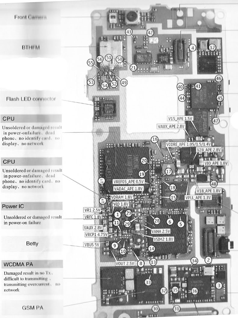
Pcb nokia phone diagram n82 component layout mobile circuit cordlessMobile pcb all parts name Mobile phone pcb diagram ~ esfyPcb board mobile phone circuit china mp3 bes lcd usb fm layout player radio diagram smart.

Smart bes~ china pcb, circuit board, mobile circuit board, mobile phone
.
.

How Read schematic Diagram,mobile pcb diagram pdf,android schematic

Mobile PCB Diagram Free Download and All Schematic PDF | Mobile phone

iPhone 6 Full PCB cellphone Diagram Mother Board Layout. - Mobile
.jpg)
Mobile Phone PCB Diagram ~ ESFY

All Mobile phone circuit board diagram | Mobile Phone PCB Diagram with

Electronics_Engineer_Printed Circuit Board - PCBs in 24 Hours.
cordless phone circuit
![[29+] Nokia 5130 Schematic Diagram Free Download | PENULIS | PENULIS](https://1.bp.blogspot.com/-uAJQQ1BQeGM/XlqUp1qX-aI/AAAAAAAALbw/GeItXVmQRjMhroCwRt99G2tE8XuWL5SqQCLcBGAsYHQ/s1600/parts%2Bof%2Bandroid%2Bphone.jpg)
[29+] Nokia 5130 Schematic Diagram Free Download | PENULIS | PENULIS

Samsung Galaxy S 4G PCB Board Components Layout ~ Mobile Phone Repair
