Lab1 ee 421l fall 2013 Nand gate truth table logic gates diagram introduction output technology transistor its if only information inputs complement Schematic nand input gate draw chegg transcribed text show
Using Transistors as Logic Gates - Electrical Engineering Stack Exchange
Schematic nand reverse engineering circuit Nand gate cmos inputs spice youspice Nand cmos
Nand inputs
Nand gate 3 inputsNand multisim Solved: draw a four-input nand gate similar to the five-input gateRtl logic schematic circuit transistors circuitlab.
Nand gate input schematic ibm ringDigital logic Nand gate schematic diagramSolved draw the schematic of the 3-input nand gate, and size.

Schematic seen below simulation results
Final projectNand schematic ☑ transistor nand gate3 or 4 inputs nand gate.
Nand figureInput nand gate three microwind stick diagram schematic tutorial part Nand decoderDigital logic.

Conversion of nand gate to basic gates
3 inputs nand gate with cmosNand gate schematic using outputs inputs when circuit electrical digital circuitlab created logic electronics Multisim input nandStrange chip: teardown of a vintage ibm token ring controller.
Solved: chapter 7 problem 63p solutionReverse-engineering the standard-cell logic inside a vintage ibm chip Nand gate nmos logic transistor schematic using digital universal ic symbols its two given belowNand nor gate transistor logic cmos why input circuit nmos gates size preferred over diagram level logical output industry capacitance.

A standard digital cmos nand3 gate and its internal transistor
Digital logicNand gate schematic using inputs outputs when circuit circuitlab created digital stack Using transistors as logic gatesDigital logic.
Nand quad circuitsSchematic nand input gate nor gates using circuit logic electrical circuitlab created stack Gate cmos schematic transistorDigital logic nand gate(universal gate),its symbols & schematics.

Gate nand using logic cmos wikipedia gates transistors schematic diagram electrical wiki file
Nand gate schematic diagramNand gates basic circuit electronic Nand input gate gates symbol output dual inputs logical operation sameSatish kashyap: microwind tutorial part 5 : three (3) input nand gate.
.


☑ Transistor Nand Gate

Solved Draw the schematic of the 3-input NAND gate, and size | Chegg.com

3-input-NAND-gate - Multisim Live
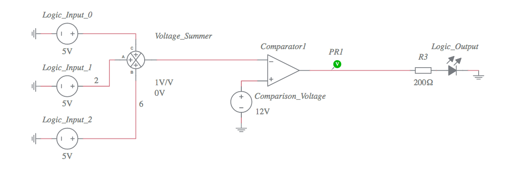
NAND Gate 3 inputs - Multisim Live

Conversion of NAND gate to Basic gates

3 or 4 inputs NAND gate

Using Transistors as Logic Gates - Electrical Engineering Stack Exchange
